(Copyright 2003, J.Kortge, K8IQY
and the American QRP Club)
Downlaod
PDF version of this Construction Guide (With thanks to Tony Fishpool,
G4WIF)
This article covers the construction and packaging of the recently released NorCal
Keyer Kit. It approaches these tasks as a learning exercise for new
builders, so that they can develop proficiency and self-confidence.The kit itself
is quite simple. It includes a printed circuit (PC) board, 7 capacitors,
4 resistors, three semiconductors, a small speaker, and a push button switch.
One of the semiconductors is a PIC microprocessor, which provides most of the
keyer’s functionality.
A few user-supplied components are required too, including a small 100K
potentiometer, jacks for input and output connections, a battery connector
or box, and a case. The kit is designed for packaging in the ever popular
Altoids mint tin.
To build this kit requires a few basic electronic hand tools. The first
is a suitable soldering iron. Anything between 25 and 40 watts is useable,
with at least a 1/16-inch wide chisel tip. However, tips that are closer to
1/8-inch will provide better heating of the joint being soldered. While a
temperature controlled soldering station is very nice, one can get by nicely
with a much more modest solder iron setup. The iron shown in figure 1 is
an inexpensive, adjustable 25-40 watt unit, and quite suitable for constructing
this type of kit.
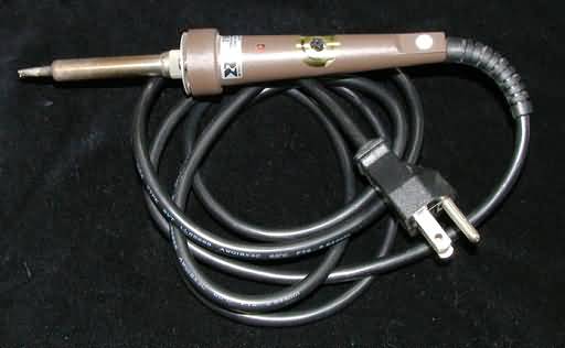
Figure 1: Soldering Iron
If you have never soldered any electronic parts, a little practice before
starting on your kit might be in order. Go to your local Radio Shack, or
other parts store, and buy a few small resistors and capacitors. If they have
any sort of perforated PC board material available, get some of that too.
You can practice putting the parts through the holes, bending the leads
slightly, and soldering them in. Do not clip off the leads; the parts can be
unsoldered and reused for more practice. If you can’t find any perforated PC
board material, buy a piece of blank PC board material, and drill several holes
in it spaced the lead width of the parts you have available, and use that for
practice. Another approach might be to take apart an old wireless telephone
and remove the existing parts by heating the PC board with a small torch and
rapping it on a solid surface to knock them out. Wear eye protection when
using this method for parts removal!
Soldering a part requires placing the tip of the soldering iron against
the component lead and the PC board surface, heating it for a few seconds,
and then adding a little bit of solder. If the joint is hot, the solder will
flow quickly. Once the solder has flowed, remove the soldering iron and the
solder, and let the joint cool. If the job was done correctly, the solder will
have flowed smoothly, and the joint will look shiny. Later in this article
are many examples of correctly soldered joints.
Solder plays a key role in electronics construction. The right kind will
work well, and is easy to use. The wrong kind can be hellish! A suitable solder
for electronics work will contain approximately 37% tin, and 63% lead. Anything
around those two values, with a rosin flux core is suitable. Do not
use “no lead” solders intended for plumbing; they will not work well. Nor will
solders with acid flux cores. Also, stay away from solders with
water-soluble (organic) fluxes. While they seem to work well while
building, failure to remove all of the flux later will lead to corrosion where
the flux remains. This is also true of any acid flux core solders.
The best solders also contain about 2% silver. This improves conductivity
of the joint, and keeps it bright looking. Figure 2 shows a small roll of
solder containing 2% silver, and readily available from Radio Shack. Kester
also makes a similar product that is available from Mouser and DigiKey.
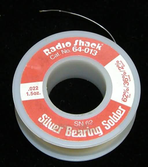
Figure 2 – Solder available from Radio Shack
The other basic tool that one needs, especially when soldering a PC board,
is a pair of side cutters. A favorite is shown in figure 3. These are
made by Xcelite, and are available from Mouser, DigiKey, and others supply
sources. These cutters are used to clip off the excess lead length of parts
soldered into the PC board.
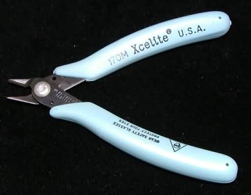
Figure 3 – Side cutters are very useful in clipping off excess lead length
Another tool that is very handy to have, but not a necessity, is a “third hand”
apparatus of some kind. A commercial version is shown in figure 4. One of
these will hold the PC board while parts are being soldered, or hold parts
while leads are being attached. One could make the equivalent of this unit
with a pair of “pincher” clothespins, a small block of wood, and a bit of
fabricating.
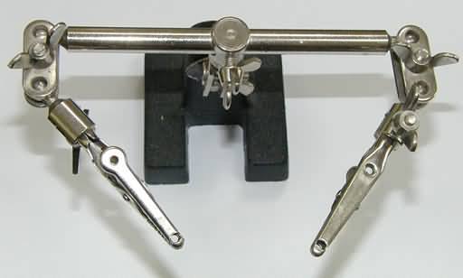
Figure 4: “Third Hand” holds PC board during assembly
Since the version of the NorCal Keyer kit I was asked to build included
the “user supplied parts”, my kit came is a box instead of an envelope.
Upon opening the box, this was what was inside. Figure 5.
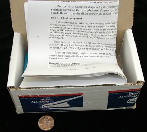
Figure 5 – Shipping box containing NorCal Keyer Kit
On the very top of the stack were the instruction sheets, shown in
figure 6. With the box (or envelope) opened, most builders are “chomping at
the bit” to get building, and want to toss the documentation aside.

Figure 6 – Assembly instructions
For a new builder, this information is important. It contains an overview
of the kit, important construction information, parts lists, a schematic
diagram, and a parts layout template for the PC board. My advice is to read
it completely, at least once before beginning construction, and the “General
Notes About Building”, “Construction Notes”, and “Parts List” a second time
before going further. When you start unpacking your kit, you will have a
good bit of sense regarding how the kit functions, and what parts were supplied.
Once the documentation has been read, it is time to unpack the rest of the
goodies. Inside the Altoids tin were the “normally supplied” kit parts, all
sealed in plastic, as shown in figure 7, …
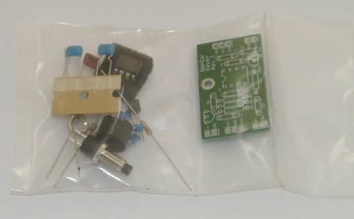
Figure 7 – Kit components sealed in plastic
and the “user-supplied parts”, loose in the Altoids tin, as shown below.
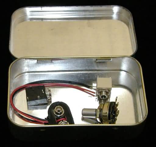
Figure 8 – User-supplied parts for kit.
With the parts packet is opened, one should check its contents against the
parts list contained in the documentation, and shown in figure 9 to make sure
all of the parts are there. If any parts are missing, replacements can be
obtained from NorCal QRP Club, Inc.
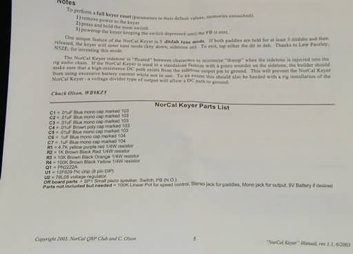
Figure 9
– Check-off
contents found in kit
When you
have build several kits, knowing what a resistor is, and determining its value
is almost taken for granted. When it
is your first kit, however, recognizing resistors, capacitors, transistors,
regulators, and PICs can be a bit daunting.
Since this article is for beginning kit builders, a number of pictures
were taken to help with this task. Using
the parts list in the supplied documentation as a guide, all of the parts in
this kit will be previewed, and their external features described.
Capacitors
C1, C2, C3, and C5 – These four capacitors have a value of 0.01 uF, are blue
in color, and marked as 103. Figure
10 shows this set of capacitors. The
103 designator translates into 10,000 pico Farad, which is the same as 0.01
micro Farad.
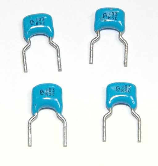
Figure 10 – C1, C2,
C3 and C5 =
“103”
Capacitor
C4 – This capacitor also has a value of 0.01 uF, is brown in color, but has a
different internal construction, making it stable with temperature changes.
It is shown below.
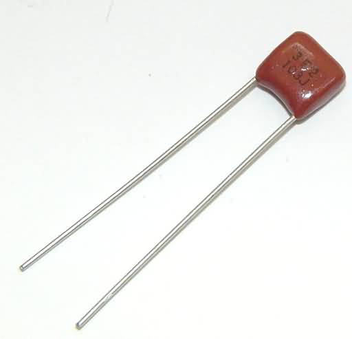
Figure 11 – C4 = 0.01
uF
Capacitors
C6 and C7 – These capacitors are much like the set with C1, only 10 times
larger in value. They have a
capacitance of 0.1 uF, are also blue in color, and marked as 104.
The 104 designator translates into 100,000 pico Farad, equivalent to 0.1
micro Farad. Figure 12shows this
capacitor pair.
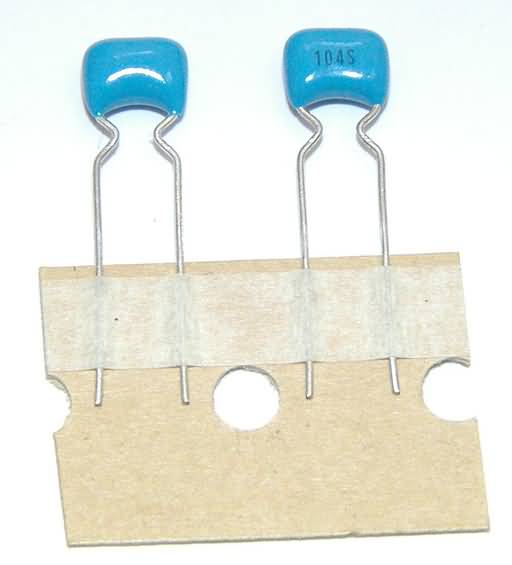
Figure 12
– C6 and C7
= “104”
This kit
contains four resistors. The first, designated R1 has a value of 4.7 kilo Ohm
(4700 Ohm), and is marked with colored bands of yellow, violet, and red.
The first two colored bands provide the first two digits of the numeric
value, the third band the multiplier, and the last band the tolerance.
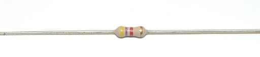
Figure 13
– R1 = 4.7
k-Ohm (yellow-violet-red)
Resistor
R2 is a 1 kilo Ohm (1000 Ohm) unit, with bands of brown, black, and red.
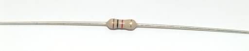
Figure 14
– R2 = 1
k-Ohm (brown-black-red)
Resistor
R3 is ten times larger than R2. It
is a 10 kilo Ohm (10,000 Ohm) unit with bands of brown, black, and orange.
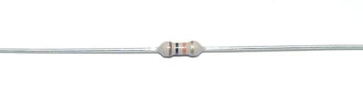
Figure 15 – R3 = 10
k-Ohm (brown-black-orange)
The last
resistor is R4, which is ten times larger than R3.
It is a 100 kilo Ohm (100,000 Ohm) unit with bands of brown, black, and
yellow, and shown in figure 16.
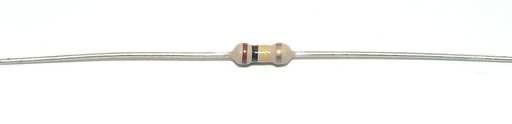
Figure 16 – R4 = 100
k-Ohm (brown-black-yellow)
By now,
you have probably figured out most of the resistor color
code.
Here it is in its entirety.
Color
Value
Black
0
Brown
1
Red
2
Orange 3
Yellow
4
Green
5
Blue
6
Violet
7
Grey
8
White
9
If you are
curious about the tolerance bands, you might try researching that information on
the Internet.
There are
three active components in this keyer. The
first is a PN2222A transistor, designated as Q1.
Figure 17 shows what this part looks like.
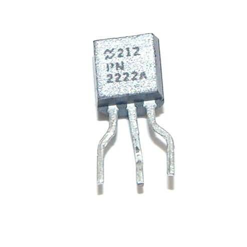
Figure 17 – Q1 =
PN2222A
The next
active component is designated as U1, and is the heart of the keyer.
U1 is the PIC microprocessor, which comes with the software, (actually
firmware) already stored in the chips memory area.
This part provides all of the functionality provided by the keyer, and is
shown in figure 18. Notice that this 8-pin DIP chip is supplied with its leads
pressed into conductive foam. This
chip is sensitive to static charge, and keeping it plugged into conductive foam
shorts all of its leads together so that it is not damaged by shipping or
handling.
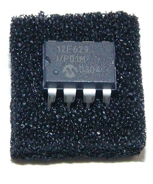
Figure 18
– U1 = PIC
microprocessor in conductive foam pad
A five
volt regulator, designated U2, is the last active part supplied with the keyer.
It is the same size and shape as the transistor.
However, the printing on it, which is difficult to read, identifies it as
a 78L05. The photograph of this
part, figure 19, was unable to clearly pickup the labeling information.
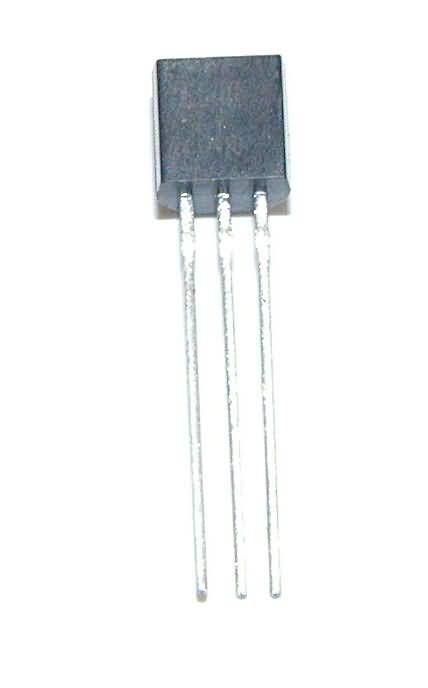
Figure 19
– 5V
regulator U2 = “78L05”
Two non-PC
board mounted parts are also included. One
is a small piezoelectric speaker, called out as SP1.
This is the same kind of speaker used in modem cards.
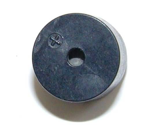
Figure 20
–
Piezoelectric speaker SP1
The other
kit supplied off board part is a small push button switch, designated as SW1 on
the schematic diagram.
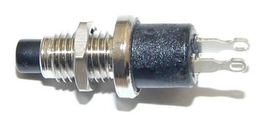
Figure 21
–
Pushbutton switch = “SW1”
Not
mentioned in the Keyer Parts List is the supplied printed circuit board.
This is a high quality, double sided board, with plated through holes,
solder mask, and silk screened parts labels.
The component side of this PC board is shown below …
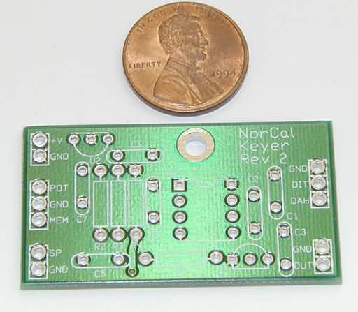
Figure 22
– Component
side of PC board
and the
solder side is shown below
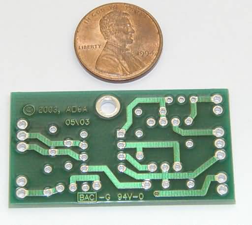
Figure 23 – Solder
side of PC board
Four
“user supplied” electronic parts are also needed to complete the keyer,
along with a suitable case for packaging the unit.
The first of these parts is a 100 kilo Ohm (100,000 Ohm) linear
potentiometer, which controls keying speed.
The potentiometer supplied for this article is shown in figure 24.
It was a 17 mm diameter potentiometer with a Ľ inch shaft, and can be
obtained from Mouser Electronics, their part number 31CN501.
Other smaller, but more expensive potentiometers are also available from
this source.
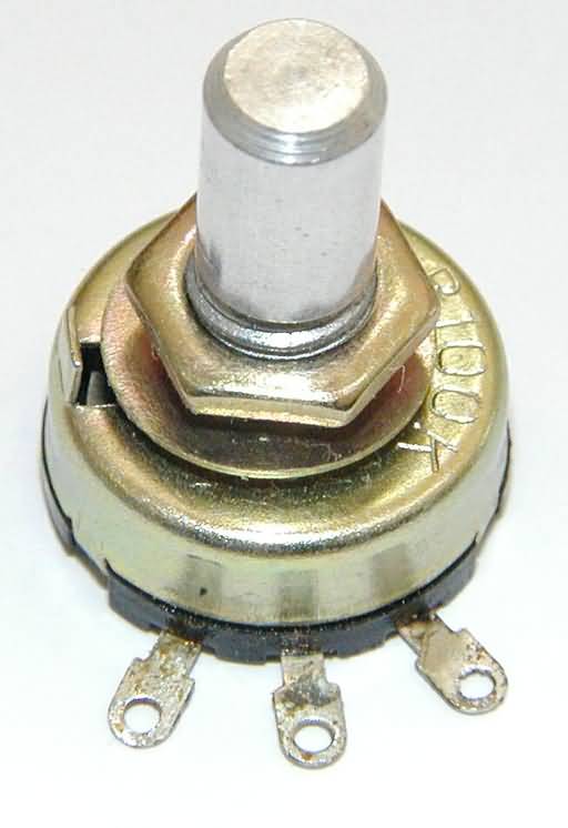
Figure 24
– 100 k-Ohm
linear-taper potentiometer
The next
part needed is a 1/8-inch, stereo jack for connecting the paddles to the keyer.
This part is shown in figure 25. It too is available from Mouser as part
number 161-3501. It might also be
available from your local Radio Shack or electronics parts store.
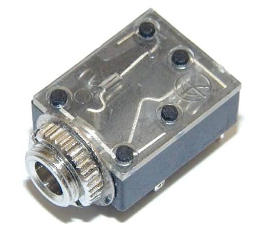
Figure 25 – 1/8”
stereo jack
A 1/8-inch
mono jack, as shown in figure 26, is also required.
This jack connects the keyer output to your transceiver, if the keyer is
being used “on the air”, instead of as a code practice oscillator.
This jack is Mouser part number 16PJ137, and may also be available at a
local electronic parts store.
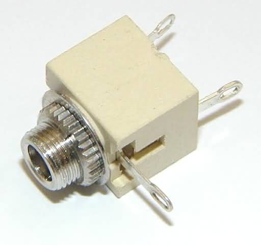
Figure 26 – 1/8”
mono jack
As
designed, the keyer is powered from a 9 volt battery, and so a battery
connector, like that shown in figure 27, is needed.
Mouser carries that part also as part number 123-6004.
Radio Shack also carries this type of connector.
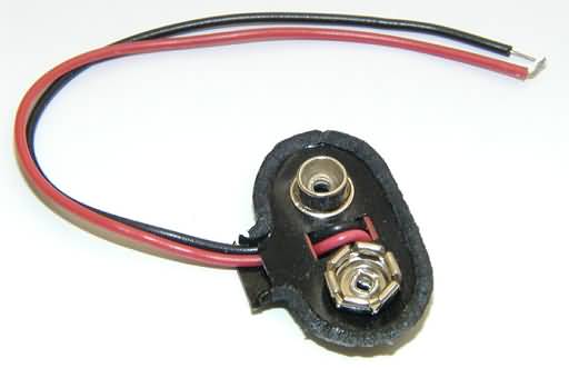
Figure 27 – 9V battery connector clip
The last
part needed is a suitable case. This
one is easy! The keyer was designed
to fit into an Altoids tin. Most
grocery stores and pharmacies carry these mints, in a variety of flavors.
Buy the flavor(s) that you like, eat them, and you have the case.
Figure 28 shows the “Wintergreen flavored” case that was supplied for
this article. Regrettably, someone
ate the contents!

Figure 28 – Altoids
mint tin used as the project case)
Enough of
the basics; it is time to build! We
will begin by soldering the parts (also called “stuffing”) into the printed
circuit board. Generally, it is best
to start with passive parts, the resistors and capacitors, and follow those with
the active parts. This approach
ensures that circuitry exists around the leads of static sensitive components,
which protects them when they are soldered.
Another good general rule to follow is to solder in the smallest parts
first. This prevents a larger part
from obscuring a smaller neighbor, which would make stuffing and soldering more
difficult. As the parts are added to
the PC board, the parts list can be used as a “check-off” sheet to assure
nothing is missed.
Following
this approach, the first part to be mounted is C1, one of the 0.01 uF, blue
colored capacitors. This parts leads
are placed through the appropriate holes in the PC board, and bent slightly
outward on the bottom side of the board to hold the part in place.
This is shown below.
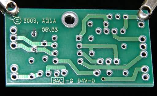
Figure 29
– Mounting
capacitor C1
The leads
are soldered, one at a time, and the excess lead length clipped off with the
side cutters, resulting in the bottom of the board looking like …
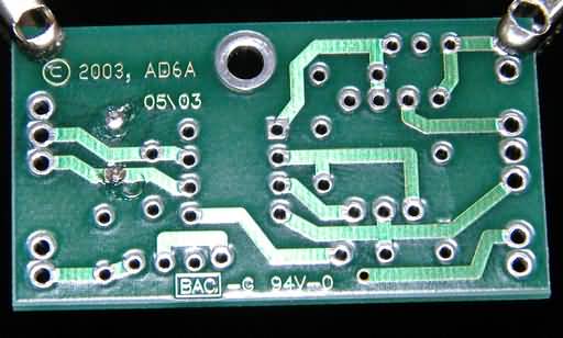
Figure 30 – Bottom of
PC board with C1 soldered in place
and the
top looking like below.
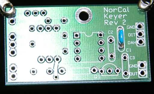
Figure 31 – Top of PC
board with C1 mounted
In like
manner, capacitors C2, C3, and C5 can be soldered in place, resulting in a PC
board which looks like that shown below.
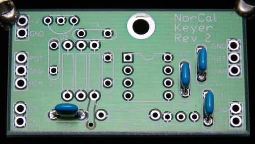
Figure 31a – PC board
with C2, C3 and C5 soldered in place
With these
parts soldered in place, check them off on the parts list, as was done below.
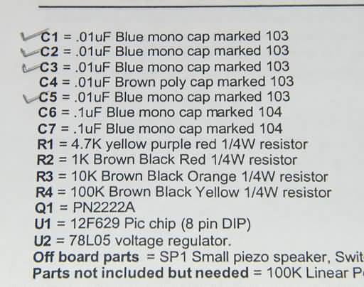
Figure 32 – Check off
the parts as you attached them to PC board
Resistors
R1 through R4 are next soldered in order. Starting
with R1, bend the leads close to the body, so that it looks as shown below.
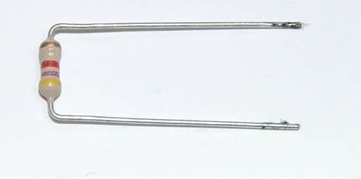
Figure 33 – R1 with
leads bent for insertion to PC board
Fingers
work well for this task, as do a small pair of long nose pliers.
Slip the part into the PC board so that the body of the resistor lays on
the surface, as shown next.
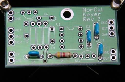
Figure 34 – R1
inserted into PC board
Bend the
leads outward as shown below and solder it.
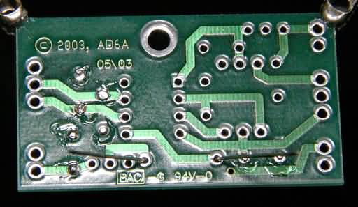
Figure 35 –
Bend
leads outward to hold
resistor close to surface of the PC board
Clip off
the leads as shown below..
Figure 36 – R1 with
leads clipped off
When the
remaining three resistors (R2 through R4) have been mounted using the same steps
as before, the board will look like this …
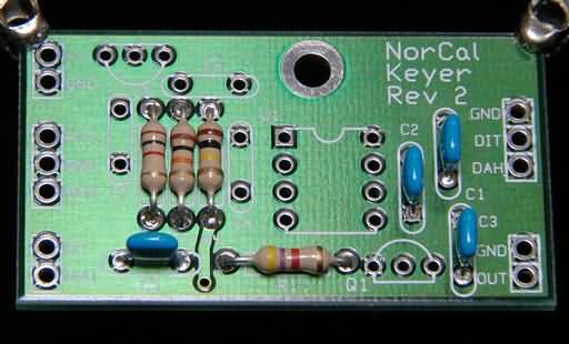
Figure 37 – All
resistors soldered in place
Check
these parts off on the parts list also, as shown here …
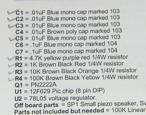
Figure 38 – Resistors
checked off the list
Following
the smaller part, larger parts approach, C4, the brown 0.01 uF capacitor is now
soldered in place. With it
installed, the board will look as shown below.
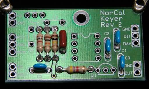
Figure 39 – Capacitor
C4 soldered in place
This part
can now be checked off on the parts list, as shown here …
Figure 40 – Check off
C4
In like
manner, solder in C6 and C7, the blue 0.1 uF capacitors, resulting in the board
looking like below …
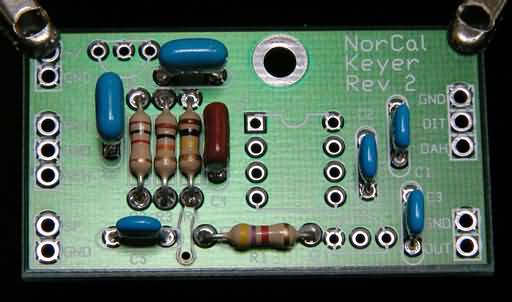
Figure 41 –
Capacitors C6 and C7 installed
and
checked off on the parts list …
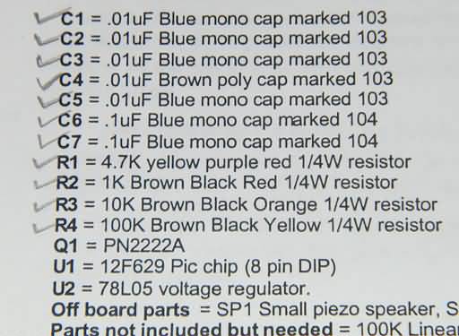
Figure 42 – C6 and C7
checked off the Parts List
Now that
all of the PC board mounted parts are in place, the active components can be
placed. Start with Q1, the PN2222A
transistor. Make sure the leads are
straight, and spaced apart to match the mounting holes.
When soldered in place, the board will look like this …
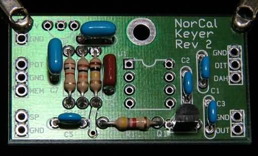
Figure 43
–
Transistor Q1 installed on the PC board
Follow
this part with the installation of U2, the 5 volt regulator.
With it installed, the board will look like this …
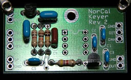
Figure 44 – The 5V
regulator, U2, is installed
Finally,
solder in the PIC chip, or preferably, use an 8 pin socket for the chip.
Using a socket allows one to easily remove this device should it fail, or
replace it if an updated version becomes available.
Make sure the device or socket is oriented properly before soldering, and
only solder two opposite pins initially. Recheck
the orientation again before soldering the remaining pins.
It is a lot easier to remove the chip or socket with two pins soldered,
and with all eight. With the chip or
socket installed, the board will look like below.
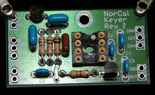
Figure 45 – Socket installed
Check off
these three active parts on the parts list, as shown here …
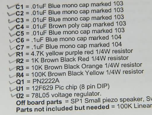
Figure 46 – Check off
Q1, U1 and U2
Finally,
if you have opted to use a socket for U1, bend the leads to fit, and plug in the
chip. The completed board will look
like this …
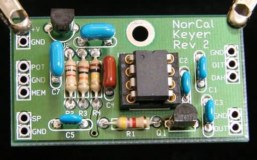
Figure 47 – The
completed board
With the
PC board finished, one more optional operation can be performed.
Using some isopropyl alcohol and an old tooth brush, clean the flux off
the solder side of the PC board. While
this step is not necessary, since the rosin flux is non-conductive, cleaning the
board makes it look much nicer, as shown here …
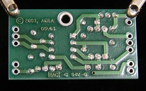
Figure 48 – Board
cleaned with isopropyl alcohol
Before the
PC board can be initially tested, two of the external parts must be attached.
First, the piezoelectric speaker, SP1 must be wired in, followed by the
battery connector. Solder a pair of
small gauge insulated wires (#26 is a good choice) about 4 inches long to the
speaker leads. A good choice for
wire are small sections of multi-conductor cable available from electronic
supply houses. An example of this
type of cable will be shown in a later picture.
Solder the other end of this pair to the appropriate holes in the PC
board. Solder in the leads from the
battery connector also.
With these
connections made, attach the battery. The
keyer should send “FB” (short for “fine business”) in Morse code at 16
words per minute (WPM). Figure 49
shows the keyer performing for this initial test.
If it does not send “FB”, follow the trouble shooting steps in the
provided documentation. Assuming
that “FB” is heard, disconnect the battery so that the remaining external
parts can be connected.
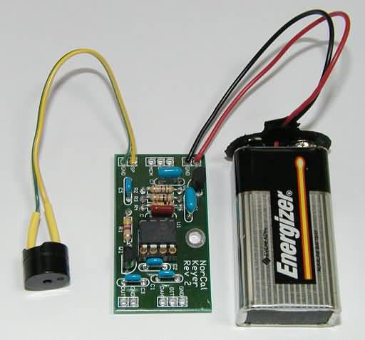
Figure 49 – Initial
tests with the Keyer
Prepare a
set of 4-inch leads for the potentiometer, VR1, as shown next.
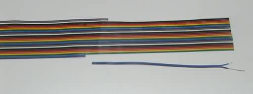
Figure 50 – Leads for
the potentiometer
Solder
these to the potentiometer terminals. Prepare
another set of leads and solder these to switch, SW1.
Photos of these parts with their attached leads are shown in figures 51
and 52.
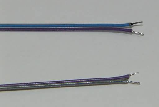
Figure 51 – Leads
for potentiometer and switch
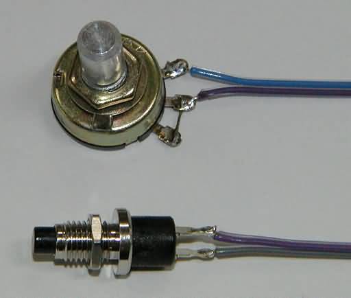
Figure 52 – Potentiometer and
switch with leads attached
Solder the
leads for these parts into their respective holes in the PC board.
The board will now look as shown below.
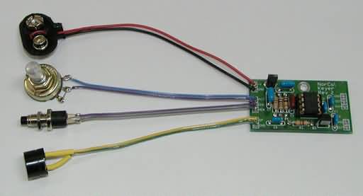
Figure 53 – PC Board
with potentiometer and pushbutton switch leads attached
Repeat the
above steps for preparing leads for the two jacks, using three leads for the
stereo jack, and two leads for the mono jack.
Solder the leads to each jack so that they look like this …
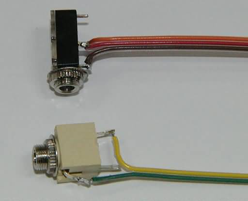
Figure 54 – Jacks
with leads attached
Solder the
respective ends to the correct holes in the PC board.
With this step completed, the PC board and external components will look
as shown below.
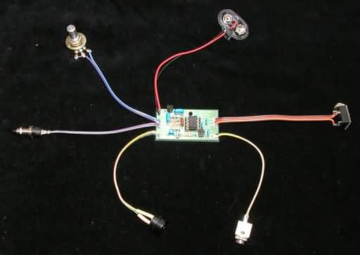
Figure 55 – Completed
PC board with external component attached
The keyer
is complete now, and ready to be fully tested, and then mounted into an
appropriate case. Those steps are
next.
Keyer Functional
Checkout
Beginning
on page two of the supplied documentation is an “Operation” discussion.
Follow what is written there to check out all of the full functionality
and capability of the keyer. Figure
56 shows the keyer, with paddles attached, during this testing.
Once satisfied that everything is working correctly, disconnect the
battery, and move on the packaging phase of this project.
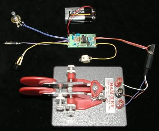
Figure 56 – Keyer
with paddles attached for testing
This
section assumes an Altoids tin will be used to house the keyer.
All controls are mounted on the front and back surfaces of the tin, to
preserve the graphics on the lid and bottom.
If another type of case is used, follow the general approach that is
described, with appropriate changes to accommodate what you have selected.
Here are
the steps that can be used …
1) Apply paper, using clear tape, over the areas where
holes will be created.
2) Mark the affixed paper where the centers of the holes
are needed, and note the required hole sizes on a sheet of paper.
The photo below shows the front of an Altoids tin, at this stage in the
process.
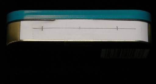
Figure 57 – Altoids
tin with paper noting hole locations
3) Punch or drill holes of the appropriate size at the
required locations. Punching holes
works better than drilling if the tools are available, as the very thin metal in
an Altoids tin tends to tear while drilling.
If drilling is the only option available, clamp a piece of wood beneath
the area to be drilled, for support.
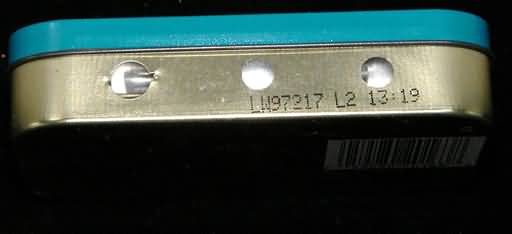
Figure 58 -
Front of the Altoids tin with the
holes now punched
4) Mount all of the external controls in their
respective holes. The output jack
was mounted on the rear panel of the tin, just below the hinge location.
5) Attach to PC board to the case floor with two small
strips of 1/8-inch thick double sided foam tape.
Super glue can be used to affix the speaker to the case top, making sure
that its leads will pass by the right edge of the PC board when the case lid is
closed. With these steps completed,
the keyer will look as shown below.
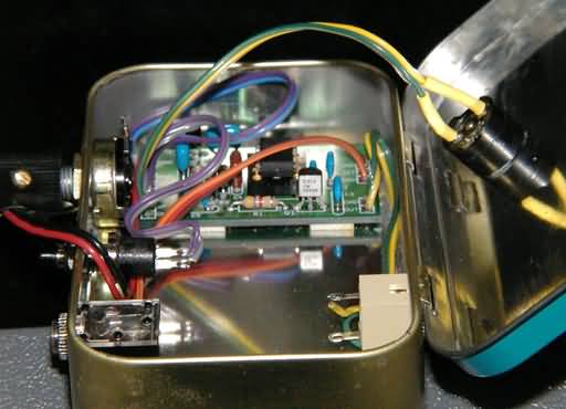
Figure 58a – Side
view of inside Altoids tin
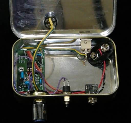
Figure 59 – inside
Altoids tin showing
components mounted
Attach the
9 volt battery to the floor of the case using a small strip of Velcro (hook and
loop) tape, so that it can be easily removed and replaced when dead.
This arrangement will also allow the battery to be removed, if the power
connector cannot be snapped off when the battery is installed.
Note that no power switch is used; disconnecting the battery fulfills
that function. With the battery
installed, the keyer looks like this …
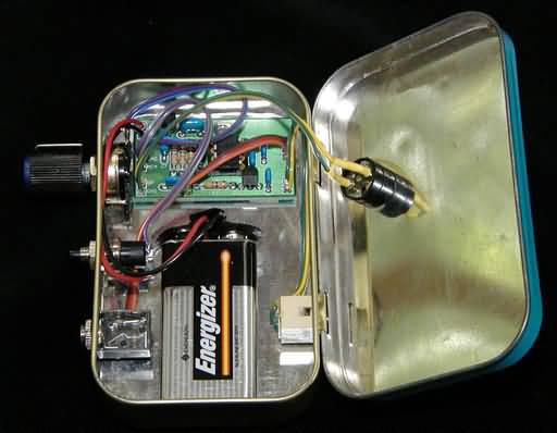
Figure 60 – Keyer in
Altoids tin with battery installed
Sharp eyed
readers will have perhaps noticed that the connections to the rear mono jack,
and the front panel mounted switch were redone.
(Look back at figure 59) These
two components originally protruded into the battery space too far, making
battery mounting impossible. Their
terminals were shortened and their wires reattached, which provided the needed
additional room.
As a final
packaging touch, small rubber feet were placed on the bottom surface at each
corner to elevate the keyer approximately 3/16-inch above its resting surface.
This provides easier access to the controls and jacks.
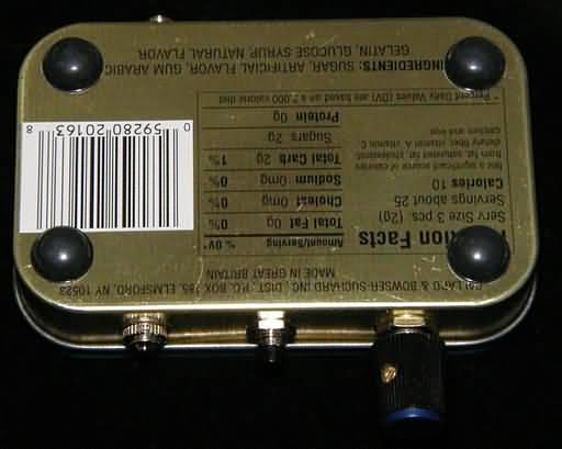
Figure 61 – Rubber
feet on bottom of Altoids tin adds a nice soft touch
The
completed keyer is shown below. No
control labeling was applied due to time constraints.
However, rub on or P-Touch ™ type
labels could be applied to the blue areas on the front and rear surfaces of the
lid, above the controls, if desired.
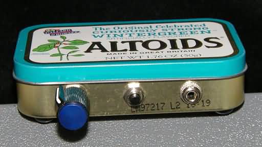
Figure 62 – Front
view of the completed NorCal Keyer
It took
about two days to build this keyer, including all of the photography that
accompanies this article.
For a beginner, that same time frame would make sense, or perhaps a day
longer. The key
is to proceed slowly and carefully, to minimize making mistakes.
Those take an inordinate amount of time to undo, and are very frustrating
for beginning builders.
Remember to read the documentation before you unpack all of the parts,
and reread the critical sections before you start building.
This keyer is an excellent beginning
builders project. It is logical to
assemble, well documented, and modestly priced.
In addition, it works wonderfully well, both for sending CW “on the
air” or in use as a code practice oscillator setup.
Either way, it is another winner from NorCal!
Hopefully, you find the information presented informative and useful.
If you have comments or questions, please contact me via email at jokortge@prodigy,
or via snail mail at my call book
address.
72 and
happy building,
Jim Kortge, K8IQY
PO Box 108
Fenton, MI 49430-0108
|